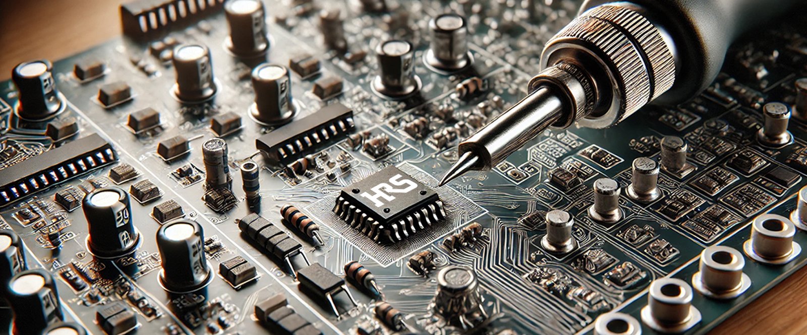
Solder is a fusible metal alloy used in electronics manufacturing to permanently join metal parts—typically component leads and PCB pads—creating both an electrical path and mechanical bond. During soldering, the solder is heated until it melts and flows between the surfaces to be joined. Upon cooling, it solidifies to form a durable joint that ensures strong electrical conductivity and mechanical stability. Proper soldering is critical for reliable performance; poor solder joints can result in weak connections, intermittent signals, or short circuits, all of which may lead to device malfunction or failure.
UNDERSTANDING MATERIALS, METHODS, AND DESIGN CONSIDERATIONS FOR RELIABLE PCB SOLDERING
Establishing a good solder joint is both an art and a science. The art lies in the skill of the operator—knowing how much solder to apply, how long to heat the joint, and being able to “feel” when a perfect bond has formed. Hand soldering relies on experience, dexterity, and intuition. The science comes into play in automated processes like reflow soldering, where precise temperature profiles, solder volumes, and timing are controlled down to fractions of a degree and second. Whether done by hand or machine, the goal remains the same: a clean, consistent, and reliable connection.
What is Solder
In technical terms, solder is a eutectic alloy—a homogeneous mixture that melts at a single, defined temperature lower than its individual constituents. This property ensures predictable melting behavior, which is essential for consistent soldering results.

Traditional solder used in electronics is typically an alloy of tin and lead. The most common formulation is 60% tin and 40% lead (Sn60Pb40), valued for its low melting point (approximately 183–190°C), excellent flow characteristics, and reliable electrical and mechanical performance. Another widely used ratio is 63% tin and 37% lead (Sn63Pb37), which forms a eutectic composition with a sharp melting point of exactly 183°C—ideal for precise, repeatable soldering.
RoHS Impact on Solder
The Restriction of Hazardous Substances (RoHS) directive, introduced by the European Union, significantly impacted solder selection in electronics manufacturing. One of its primary restrictions is the use of lead (Pb) in electronic and electrical equipment due to environmental and health concerns.
As a result, manufacturers transitioned from traditional tin-lead solders to lead-free alternatives. The most common lead-free alloy is a combination of tin, silver, and copper (Sn-Ag-Cu), which offers good electrical performance but melts at a higher temperature—typically around 217–221°C.
This shift required updates to soldering equipment, reflow profiles, and board-level designs to accommodate the increased thermal demands. Additionally, component and PCB materials had to be evaluated for compatibility with the higher reflow temperatures associated with lead-free processes.
FLUX
Flux is a critical chemical agent in electronics soldering that improves the quality and reliability of solder joints. Its primary roles are to remove oxides from metal surfaces, prevent further oxidation during the soldering process, and promote even wetting of the solder across contact areas.
Flux can be applied separately or integrated directly into solder wire as a core (e.g., rosin-core solder), allowing for continuous application during the soldering process. The use of flux ensures proper bonding between the component lead and the PCB pad, which is essential for electrical conductivity and long-term reliability.
There are three main types of flux used in electronics manufacturing:
- Rosin-Based: Derived from pine resin, it effectively removes oxides but often leaves residue that may require cleaning.
- Water-Soluble: Contains organic acids, highly active, and must be cleaned post-soldering—ideal for high-reliability applications.
- No-Clean: Leaves minimal, non-corrosive residue, reducing the need for cleaning and supporting high-volume automated production.
Choosing the right flux depends on the soldering method, cleanliness requirements, and board materials. Proper flux use is essential for minimizing defects and achieving reliable solder joints.
Solder Application
Flux is a critical chemical agent in electronics soldering that improves the quality and reliability of solder joints. Its primary roles are to remove oxides from metal surfaces, prevent further oxidation during the soldering process, and promote even wetting of the solder across contact areas.
Flux can be applied separately or integrated directly into solder wire as a core (e.g., rosin-core solder), allowing for continuous application during the soldering process. The use of flux ensures proper bonding betwee
In electronics manufacturing, soldering is typically performed using one of three methods:
- Reflow Soldering: Solder paste is applied to PCB pads, components are placed, and the board is passed through a reflow oven. The controlled temperature profile melts the solder, forming strong, reliable joints. This is the primary method for surface-mount technology (SMT) due to its precision and scalability.
- Wave Soldering: Used mainly for through-hole components, the PCB passes over a wave of molten solder. It enables fast, simultaneous soldering of multiple joints, making it ideal for high-throughput production..
- Hand Soldering: Performed manually using a soldering iron. It’s typically used for prototyping, rework, or low-volume assemblies where automated equipment isn't practical.
Each method requires proper temperature control, flux selection, and component compatibility to ensure consistent solder joint quality.
Solder Wetting
Solder wetting is the process where molten solder spreads across and adheres to a metal surface, forming a smooth, continuous bond. Proper wetting ensures the solder fuses to both the PCB pad and the component lead, creating a reliable electrical and mechanical connection.
Good wetting is essential for long-term performance, helping joints withstand thermal cycling, vibration, and mechanical stress. Poor wetting can result in weak or intermittent connections.
Wetting is also easy to inspect visually—well-formed joints appear shiny, smooth, and concave, while dull, uneven, or ball-shaped joints may indicate a problem.
Solder Wicking
Solder wicking is the unwanted movement of molten solder away from its intended location—typically from the pad up the component lead or into vias and adjacent traces. Instead of forming a solid joint at the pad, solder travels elsewhere, leaving behind insufficient material for a reliable connection. This can weaken joints, cause open circuits, or create solder bridges that lead to shorts.
In high-density assemblies, wicking can also result in bumps or solder buildup on the opposite side of the board, affecting board flatness and reworkability.
Primary causes of solder wicking include:
- Thermal Imbalance: If the lead or another area heats up faster than the pad, solder will naturally flow toward the hotter region.
- Surface Finish and Wetting Issues: When solder wets the component lead faster than the pad, solder is drawn away from the intended joint.
- Unmasked Vias and Traces: Vias or exposed copper areas not protected by solder mask act as unintended solder pathways.
- Contamination or Poor Surface Prep: Oxidized, dirty, or poorly plated surfaces hinder wetting and encourage solder to wick away.
Solder wicking compromises both mechanical and electrical performance, making prevention a key consideration in PCB and connector design
Preventing Solder Wicking
Hirose incorporates multiple design strategies across its connector families to proactively prevent solder wicking and maintain high connection reliability—even in fine-pitch or high-density assemblies.
Key anti-wicking design features include:
- Nickel-Plated Barriers: Many series, including DF40 and TF43SW, use nickel barrier plating on terminal leads. This plating acts as a physical and chemical barrier that blocks solder migration into the contact area, preserving electrical integrity and reducing the risk of shorts.
- Molded Anti-Wicking Structures:
Hirose uses various molding techniques to eliminate gaps between terminals and housings, blocking solder migration into sensitive areas. These include:- Integrally Molded Structures: Series like BK13 feature plug and receptacle parts formed as a single molded unit, eliminating spaces where solder could flow into contact zones.
- Insert Molded Headers and Receptacles: In series such as KN13C, terminals are tightly sealed into the housing during molding—especially effective for miniaturized or fine-pitch designs.
- Molded-In Contacts: In the DF61 series, contacts are embedded directly into the insulating housing to physically prevent solder wicking during reflow.
- External Walls and Housing Features: Some Hirose connectors include structural elements—such as walls or indentations—which protect exposed contact areas from solder intrusion and also shield against flux or foreign particles.
- Design for Assembly: Hirose also supports solder wicking prevention through careful layout, including solder mask dams, optimized pad geometry, and precise terminal shaping to help guide solder flow.

By combining smart material selection with form factor engineering, Hirose ensures solder stays exactly where it’s intended—delivering consistent, high-reliability connections in automated and manual soldering environments.
Conclusion
Solder wicking poses a serious risk to connection integrity—particularly in modern electronics where space is limited and components are densely packed. Hirose addresses this challenge through a range of connector design strategies, including nickel barrier plating, molded-in contacts, and sealed terminal structures. These features work together to contain solder flow, protect critical contact areas, and support high-reliability performance across various soldering methods.
By engineering connectors to prevent solder intrusion at the design level, Hirose helps manufacturers ensure stronger, cleaner solder joints, ultimately improving yield, reducing rework, and enhancing long-term reliability in demanding applications.
connection point
Welcome to 'Connection Point' - your go-to spot for the latest in electronics. Here, we're all about connecting you with fresh ideas, engaging stories, and innovative solutions from Hirose Electric. Whether you're a tech enthusiast or an industry professional, there's something here for everyone.
Don't miss out on any of our updates – subscribe now and join our community of innovators and thinkers.
For more information on how Hirose Electric's connectors can transform your wearable device design, visit hirose.com or contact our team of experts today.